Avoid Defects in the Powder Bed Fusion Process with Printability Maps

Image 1. Printability map created experimentally for Ti-6Al-4V (left) and a printability map simulated in the AM Module for 316L (right). Both printability maps show possible defects based on power and scan speeds for their relative materials, with defects in the upper left and lower right corners and and full density in the center. The left image is reprinted from Additive Manufacturing, Vol 48, part A, Jenniffer Bustillos, Jinyeon Kim, Atieh Moridi, Exploiting lack of fusion defects for microstructural engineering in additive manufacturing, 2021, with permission from Elsevier. https://doi.org/10.1016/j.addma.2021.102399
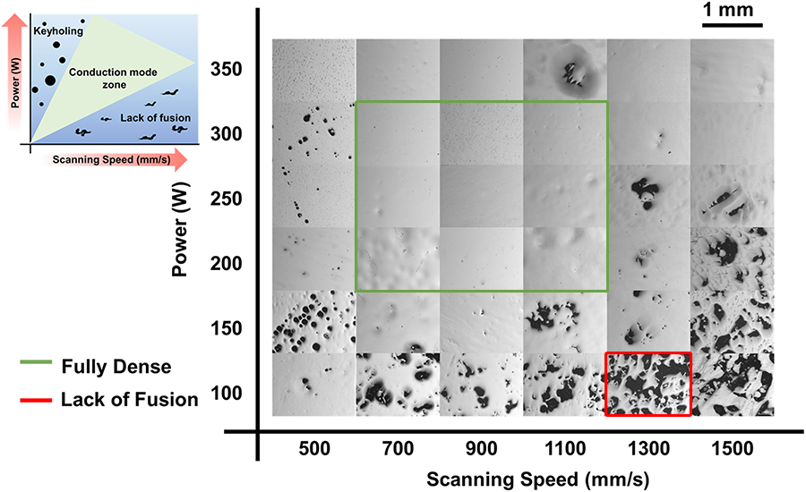
Image 2. A printability map, also known as a processing map, of Ti-6Al-4V showing possible defects based on power and scan speed combinations. Lack of fusion can be seen in the bottom right corner (red), keyholing in the top left corner, and full density in the center (green). Reprinted from Additive Manufacturing, Vol 48, part A, Jenniffer Bustillos, Jinyeon Kim, Atieh Moridi, Exploiting lack of fusion defects for microstructural engineering in additive manufacturing, 2021, with permission from Elsevier. https://doi.org/10.1016/j.addma.2021.102399
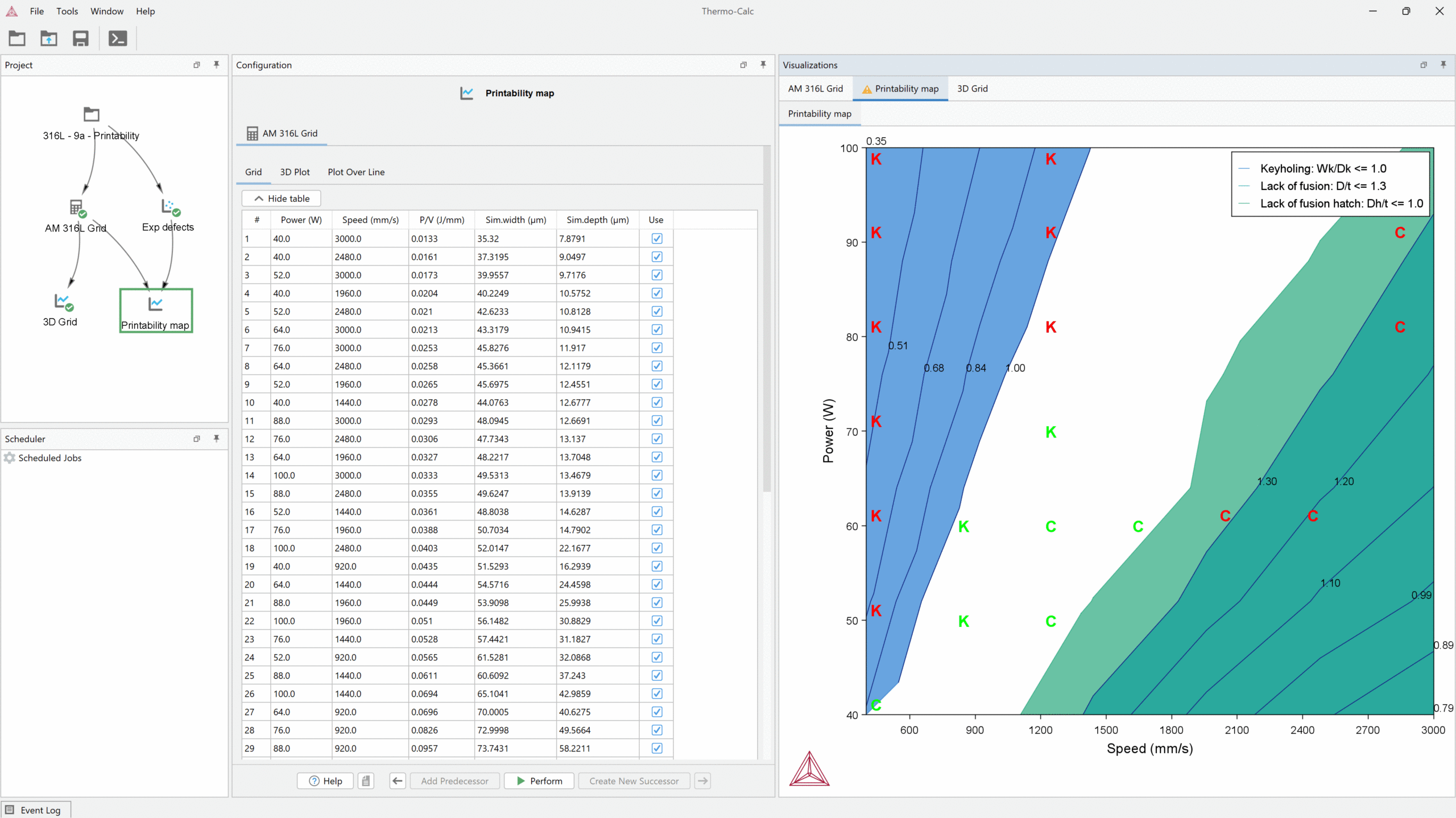
Image 3. A printability map calculated in the AM Module for the material 316L showing the power and scan speeds that are likely to result in keyholing (blue area) and lack of fusion (green area). The white area shows the power and scan speeds that are optimal to reduce the risk of these defects.